Quantcast
Channel: News & Updates - PIC Microcontroller
Viewing all 3566 articles
Browse latest View live

ULTRA-LOW QUIESCENT LDO EXTENDS BATTERY LIFE FOR SENSORS AND PORTABLE DESIGNS

$
0
0

With ultra-low quiescent current of 250 nA, the MCP1811 enables battery life which is four-times longer than conventional ultra-low Iq LDO regulators. Compact packages down to 1 x 1 mm also help the MCP1811 to minimise board space.

ULTRA-LOW QUIESCENT LDO EXTENDS BATTERY LIFE FOR SENSORS AND PORTABLE DESIGNS

The MCP1811/12 devices are 150 mA (MCP1811) and 300 mA (MCP1812) low dropout (LDO) linear regulators that provide high-current and low-output voltages while maintaining an ultra-low 250 nA of quiescent current during device operation. In addition, the MCP1811B/12B can be shut down for 5 nA (typical) supply current draw.

The MCP1811/12 family comes in nine standard fixed output-voltage versions: 1V, 1.2V, 1.8V, 2.0V, 2.5V, 2.8V, 3.0V, 3.3V, and 4.0V. The 150/300 mA output current capability, combined with the low output-voltage capability, make the MCP1811/12 device family a good choice for new ultra-long-life LDO applications that have high-current demands, but require ultra-low power consumption during sleep periods.

The MCP1811/12 is stable with ceramic output capacitors that inherently provide lower output noise and reduce the size and cost of the entire regulator solution. Only 1 μF (2.2 μF for MCP1812) of output capacitance is needed to assure the stability of the system with a low noise output.

Block Diagram

Additional Features

  • Ultra-Low Quiescent Current: 250 nA (typical)
  • Ultra-Low Shutdown Supply Current: 10 nA typ (MCP1811A) and 5 nA typ (MCP1811B)
  • Input Voltage Range: 1.8V to 5.5V
  • Standard Output Voltages: 1.0V, 1.2V, 1.8V, 2.0V, 2.5V, 2.8V, 3.0V, 3.3V and 4.0V
  • Low Dropout Voltage: 400 mV (typical) w/ Small Variation Over Load Range
  • Stable with Ceramic Output Capacitor: 1.0 uF
  • Overcurrent Protection w/ Foldback
  • Output Discharge (MCP1811A)
  • Available in 3 and 5 lead SOT-23, 3 and 5 lead SC70, 4 lead 1x1mm UDFN

Read more: ULTRA-LOW QUIESCENT LDO EXTENDS BATTERY LIFE FOR SENSORS AND PORTABLE DESIGNS

The post ULTRA-LOW QUIESCENT LDO EXTENDS BATTERY LIFE FOR SENSORS AND PORTABLE DESIGNS appeared first on PIC Microcontroller.


Newly Developed Internal Temperature Sensor For Li-ion Battery Enables 5x Faster Charging

$
0
0

Researchers at the University of Warwick in the UK have developed sensors which measure the internal temperature and electrode potential of Lithium batteries. The technology is being developed by the Warwick Manufacturing Group (WMG) as a part of a battery’s normal operation. More intense testings have been done on standard commercially available automotive battery cells.

Newly Developed Internal Temperature Sensor For Li-ion Battery Enables 5x Faster Charging

If a battery overheats it becomes a risk for critical damage to the electrolyte, breaking down to form gases that are both flammable and can cause significant pressure build-up inside the battery. On the other hand, overcharging of the anode can lead to Lithium electroplating, forming a metallic crystalline structure that can cause internal short circuits and fires. So, overcharging and overheating of a Li-ion battery is hugely damaging to the battery along with the user.

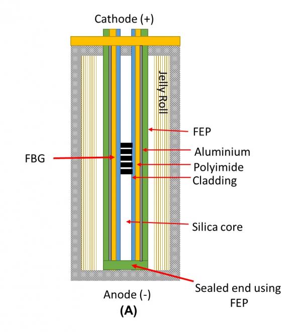
The researchers at Warwick developed miniature reference electrodes and Fiber Bragg Gratings (FBG) threaded through a strain protection layer. An outer coat of Fluorinated Ethylene Propylene (FEP) was applied over the fiber, ensuring chemical protection from the corrosive electrolyte. The end result is a sensor which has direct contact with all the key components of the battery. The sensor can withstand electrical, chemical and mechanical stress faced during the normal operation of the battery while still giving accurate temperature and potential readings of the electrodes.

The device includes an in-situ reference electrode coupled with an optical fiber temperature sensor. The researchers are confident that similar techniques can also be developed for use in pouch cells. WMG Associate Professor Dr. Rohit Bhagat said,

Read more: Newly Developed Internal Temperature Sensor For Li-ion Battery Enables 5x Faster Charging

The post Newly Developed Internal Temperature Sensor For Li-ion Battery Enables 5x Faster Charging appeared first on PIC Microcontroller.

4KOPEN – 4K UHD VIDEO DEVELOPMENT PLATFORM FEATURES STMICRO STIH418 MEDIA PROCESSOR

$
0
0

4Kopen has showcased at 2019 Integrated Systems Europe (ISE 2019) at the beginning of the month a new 4K capable board featuring STMicro STiH418 Media Processor. The development board comes with 2 GB RAM, HDMI 2.0 output, HDMI 1.4 input, Gigabit Ethernet, USB 3.0, a mini PCIe slot fitted with an 802.11b/g/n WiFi module, an eSATA connector and more.

4KOPEN – 4K UHD VIDEO DEVELOPMENT PLATFORM FEATURES STMICRO STIH418 MEDIA PROCESSOR

The board is a fully open source 4K development platform with OrCAD and PDF schematics, Gerber files, and datasheet all available for download. There’s also a Wiki explaining how to get started with Raspbian or buildroot built Starkl Linux distributions, and how to use the GStreamer media APIs

Connections

4Kopen (B2264) Hardware Specifications

  • SoC – STMicro STiH418 quad-core Arm Cortex-A9 processor @ 1.2 GHz,  quad-core Mali-400 GPU, and 4x ST231 DSP (Each Core Quad issue) @ 650 MHz
  • System Memory – 2 GB DDR3 @ 2133 MHz
  • Storage – micro SD socket, eSATA port
  • Video & Audio I/O
    • Output – HDMI 2.0 Tx up to 2160p60, 3.5mm AV jack with composite video and stereo audio
    • Input – HDMI 1.4 Rx up to 2160p30
  • Video Decode/Encode
    • Ultra HD Decoding, up to 2160p60
    • Full HD Encoding, up to 1080p60
  • Networking – Gigabit Ethernet, 802.11b/g/n WiFi 4
  • USB – 1x USB 3.0 port, 2x USB 2.0 ports
  • Expansion
    • Mini PCIe slot (wireless module included)
    • 40-pin GPIO header
  • Debugging – JTAG header
  • Misc – Reset button
  • Power Supply – 12V DC
  • Dimensions – TBC

Read more: 4KOPEN – 4K UHD VIDEO DEVELOPMENT PLATFORM FEATURES STMICRO STIH418 MEDIA PROCESSOR

The post 4KOPEN – 4K UHD VIDEO DEVELOPMENT PLATFORM FEATURES STMICRO STIH418 MEDIA PROCESSOR appeared first on PIC Microcontroller.

PacketMonitor32 – An ESP32-Based Packet Monitor with OLED

$
0
0

Wi-Fi Packet Monitors are usually a computer program or sometimes a piece of computer hardware that can be used to intercept and log traffic over a Wi-Fi network. My favorite software tool of all is the popular Wireshark which I have used several times for hacking Wi-Fi based hardware, like integrating the common Wi-Fi smart socket with OpenHAB. Packet monitor tools give the possibility of seeing what type of data is being sent out by a wireless device and provides us with the chance of conjoining that data for our purpose.

PacketMonitor32 – An ESP32-Based Packet Monitor with OLED

Apart from the use of software for packet capture, we can also leverage hardware for this. The Espressif Systems ESP8266 and the ESP32 modules have been a go-to module for a lot of makers regarding Wi-Fi/IoT applications. Stefan Kremser aka Spacehuhn who first launched an Esp8266 based packet monitor, earlier last year has released an improved opensource ESP32-based packet monitor which is available on Tindie and Aliexpress for purchase.

The original Packet Monitor board put together by Spacehuhn is based around the ESP8266 and allowed you to see data packets flying around you in real-time. It tells how many Wi-Fi packets are sent every second and on which channel. It is also able to display the result on a small OLED Screen. The ESP32 version comes with some new features.

Then new ESP32 Packet monitor includes some new features to the existing ESP8266 Packet monitor. It adds an SD card support for capturing and saving traffic data with the possibility analyzing that data at other time, unlike the ESP8266 which shows only the current packet only, the ESP32 version displays an average RSSI (Received Signal Strength Indicator), and of course offer an improved performance due to the increased power of ESP32. It is built around the ESP32-Wrover module, which has 4MB Flash and 4MB PSRAM.

Read more: PacketMonitor32 – An ESP32-Based Packet Monitor with OLED

The post PacketMonitor32 – An ESP32-Based Packet Monitor with OLED appeared first on PIC Microcontroller.

VARISCITE REVEALS AN EXTENDED PORTFOLIO OF NEW I.MX BASED BOARDS

$
0
0

Variscite reveals the portfolio of its new i.MX based products that will be presented next week at the Embedded World 2019 exhibition & conference. Variscite is the only NXP partner who was granted early access to all i.MX 8 programs and will present next week a respectable number of new System-on-Modules based on i.MX 8M Minii.MX 8QM and i.MX 8X as well as the i.MX 8M that was released in 2018.

VARISCITE REVEALS AN EXTENDED PORTFOLIO OF NEW I.MX BASED BOARDS

Alongside the i.MX 8 platforms, the company will also showcase the VAR-SOM-6UL, its new member to the ‘VAR-SOM pin2pin family’ based on NXP i.MX 6UltraLite / 6ULL / 6ULZ processors.

The Official Launch Of The DART-MX8M-MINI

The DART-MX8M-MINI System-on-Module (SoM) will be officially launched at the upcoming Embedded World exhibition. The DART-MX8M-MINI is a miniature SoM based on NXP’s i.MX 8M Mini processor with up to 2GHz Quad-core ARM Cortex-A53 plus 400MHz Cortex-M4 real-time processor. The SoM offers integrated HW engines supporting 1080p video encode and decode, 2D and 3D graphics, HQ audio and a wide range of connectivity options such as Wi-Fi/BT, Ethernet, and USB.

The DART-MX8M-MINI joins Variscite’s ‘DART Pin2Pin Family’ and provides a pin2pin scalable option to Variscite’s DART-MX8M with lower power consumption and higher CPU performance. Later this year the company is expected to launch the DART-MX8M-NANO based on the upcoming NXP i.MX 8M Nano processor for further cost/performance scalability of the ‘DART Pin2Pin Family’.

The VAR-SOM Pin2Pin Family

The company is expanding its ‘VAR-SOM Pin2Pin product Family’ with several new products which will be presented at the Embedded World exhibition: The VAR-SOM-MX8, VAR-SOM-MX8X and VAR-SOM-6UL. The Pin2Pin family offers Variscite’s customers a high level of scalability, extended lifetime availability and reduced development time, cost and risk.

Read more: VARISCITE REVEALS AN EXTENDED PORTFOLIO OF NEW I.MX BASED BOARDS

The post VARISCITE REVEALS AN EXTENDED PORTFOLIO OF NEW I.MX BASED BOARDS appeared first on PIC Microcontroller.

A combined MSF/DCF atomic clock receiver

$
0
0

For this to work you must obviously live in an area that can receive both signals. My circuit is based on two modules taken from two radio clocks bought at Lidl’s supermarket. Originally both were for the DCF clock but by substituting the original 77.5kHz crystal with a 60kHz crystal, one of the modules was converted to MSF.

Notice that both antennas are lined up in my photograph. This is because Anthorn and Mainflingen – as seen from Limavady – are roughly in the same direction. The alignment of the ferrite rods obviously has to be adapted to your location.

A combined MSF/DCF atomic clock receiver

Circuit description 

The circuit is based on the single clock projects found elsewhere on this site. The supply for the two actual receiver modules makes use of a 3.3V zener diode. Supply voltage is 5V. The four links allow both the output signals and the LEDs to be inverted by moving the link. Each group of four NOT gates – on the pcb – consists of two 7400 NAND gates wired as Not gates.

I found that the circuit worked extremely well and reception is near perfect under most conditions.

The program

I have written a simple little single tasking graphics program which plots the output of both clocks one over the other. The MSF clock is yellow, the DCF clock is green. On the right is a small section of the output.

Not much can be learned. The most interesting bits are the beginning of minute markers. This is a half second ON for the MSF clock and a full second OFF for the DCF clock. Notice also the double pulse in first DCF second indicating a 100ms difference between atomic time and GMT. This used to be 400ms not all that long ago.

A combined MSF/DCF atomic clock receiver

I have highlighted the interesting bits. Anything you see in red was not produced by my program but inserted via !Draw.

Here is a link to a zip file containing the draw file of the pcb layout, the circuit diagram and the BASIC V program below.

Version 2 of the program allows you to plot continuously or screen after screen. You can also change the time base.

For more detail: A combined MSF DCF atomic clock receiver

The post A combined MSF/DCF atomic clock receiver appeared first on PIC Microcontroller.

A DIY FLUXGATE MAGNETOMETER BASED CURRENT PROBE

$
0
0

Introduction

Current measurement can be really awkward when working with circuits. Voltage measurements are (usually) straightforward, but when it comes to current measurements the story is different. One typical approach is to insert a known resistance by breaking the circuit, and then measuring the voltage across it. This is difficult if one end of the resistor is not at ground potential, because oscilloscope probes are (usually) designed with the ground leads all connected together, and it will damage things if the grounds of different channels on the oscilloscope are connected to different parts of the circuit.

A DIY FLUXGATE MAGNETOMETER BASED CURRENT PROBE

This project describes a very sensitive home-made current probe that doesn’t require a known resistance to be inserted. It has not been fully characterized but the initial results are reasonably promising. It was tested at currents of the order of single-digit microamps up to 10mA (it can be assembled for higher current ranges if desired), and it functions from DC to around 20kHz, and is fully isolated.

It is based around a very exotic magnetic field sensor known as a fluxgate magnetometer. Ordinarily this is quite difficult to build due to the requirement for hard-to-find mu-metal and a mix of analog and digital electronics. However, Texas Instruments offers an entire fluxgate magnetometer-on-a-chip and an evaluation board. With some effort it is possible to build a current sensor or probe with it. It makes a handy test tool for measuring current in a circuit, in a less intrusive way than normal.

What is a Fluxgate Magnetometer?

There are several ways to make magnetic field sensors, and the fluxgate magnetometer offers very impressive sensitivity. There are slightly different topologies of fluxgate magnetometers, but in a nutshell they consist of windings around a core. If we use a Lego wheel tyre to act as a pretend core then ‘Excitation’ and ‘Sense’ windings can be placed around it as shown in the photo (the windings are the yellow and green wires in the photo).

Read more: A DIY FLUXGATE MAGNETOMETER BASED CURRENT PROBE

The post A DIY FLUXGATE MAGNETOMETER BASED CURRENT PROBE appeared first on PIC Microcontroller.

3.5A Unipolar Stepper Motor Driver

$
0
0

Unipolar stepper motor driver can drive unipolar motor up to 3.5A and supply range 10 To 50V DC. The board has been designed using STK672-442AEN IC.  The STK672-442AN is a hybrid IC for use as a unipolar, 2-phase stepper motor driver with PWM current control and Micro-stepping.

3.5A Unipolar Stepper Motor Driver

Features

  • Supply Up to 50V DC Input
  • Logic Supply 5V DC Input
  • Load Current 3.5Amps
  • Stepper Motor: 5 Wires, 6 Wires, 8 Wires (Unipolar)
  • Built-in over current detection function, over heat detection function (Output Off)
  • Fault 1 signal ( Active Low) is output when overcurrent or over heat is detected
  • Fault 2 signal is used to output the result of activation of protection circuit detection at 2 levels.
  • Built-in power on reset function
  • A Micro-step sin wave driven driver can be activated merely by inputting an external clock.
  • The Switch timing of the 4-phase distributor can be switched by setting an external pin (Mode3) to detect either the rise or fall, or rise only, of clock input.
  • The Enable pin can be used to cut output current while maintaining the excitation mode.
  • With a wide current setting range, power consumption can be reduced during standby.
  • No Motor noise during hold mode due to external excitation current control.
  • Incorporating a current detection resistor (0.122Ω: resistor tolerance 2%), motor current can be set using two external resistors.
  • Phase is maintained even when the excitation mode is switched. Rotational direction switching function
  • External pins can be used to select 2, 1-2 (including pseudo-micro), W1-2, 2 W1-2, or 4W1-2 excitation.
  • Clock Input : Input frequency 20Khz when using both edge, Or 50Khz when using one edge
  • Minimum pulse width 20us When using both edge Or 10us when using one edge
  • M3: Jumper J3-Open the excitation phase moves one step at a time at the rising edge of the CLOCK pulse.
  • M3: Jumper J3-Closed the excitation phase moves alternately one step at a time at the rising and falling edges of the CLOCK pulse.
  • Do not Change direction during the 7us interval before and after the rising and falling edges of CLOCK input.
  • Enable : Normally High for Normal Operation, Pull down control of excitation drive output A, AB, B, and BB, and selecting operation/hold status inside the HIC

Read more: 3.5A Unipolar Stepper Motor Driver

The post 3.5A Unipolar Stepper Motor Driver appeared first on PIC Microcontroller.


“SWORDTAIL” I.MX6 SBC OFFERS NIMBLELINK CELLULAR EXPANSION

$
0
0

Low power Arm-based i.MX6 Cortex®-A9 processor with soldered-on RAM, Gigabit Ethernet, Wi-Fi, Bluetooth® and fanless operation.

“SWORDTAIL” I.MX6 SBC OFFERS NIMBLELINK CELLULAR EXPANSION

The Swordtail single board computer is a complete Wi-Fi and Bluetooth®enabled, Arm®-based embedded computer. Models are available with power-efficient, dual-core or quad-core i.MX6 CPUs. These boards are designed for applications that demand rugged, power-efficient solutions such as industrial machine automation, transportation, medical, kiosk, and industrial IoT applications. Swordtail boards have been designed to enable transactions and transmission of maintenance or diagnostic information without the presence of a wired data connection. Both Wi-Fi and Bluetooth radios are included on board, and a NimbleLink Skywire™ socket supports a wide range of optional cellular and other wireless plug-ins.

Unlike Arm-based “modules”, Swordtail is a complete board-level computer. Additional carrier boards, connector boards, or I/O expansion boards are not required for operation. Swordtail boards are delivered with on-board soldered-down RAM, ready to plug-in and run. To simplify mounting and future upgrades, the Swordtail leverages the COM-Express standard for its footprint and mounting points.

The Following Specifications Were Listed For The Swordtail SBC

  • Processor — NXP i.MX6 Quad or DualLite (4x or 2x Cortex-A9 cores @ up to 800MHz); Vivante GC2000 GPU
  • Memory/storage:
    • 1GB (DualLite) or 2GB (Quad) DDR3L SDRAM soldered, with up to 4GB optional
    • MicroSD slot (bootable) with optional 8GB card containing Linux
    • eMMC (MLC) socket with up to 32GB optional bootable storage
  • Wireless:
    • Single-band 802.11b/g/n and Bluetooth 4.2
    • NimbleLink Skywire socket (20-pin) for cellular and other wireless expansion
    • Optional antennas
  • Networking — Gigabit Ethernet port with network boot, latching connector
  • Media I/O:
    • HDMI v1.4 port with audio
    • 24-bit LVDS for up to 1366 x 768 with backlight and I2C touch (with interrupt input)
  • Other I/O:
    • 2x USB 2.0 host ports
    • CAN 2.0B
    • RS-232 debug
    • 8x GPIO/DIO (3.3V)
    • I2C
    • Up to 3x PWM (reduces GPIO lanes)
  • Other features — 6-axis accelerometer/magnetometer; 10-year lifecycle support; optional cables
  • Operating temperature — -40 to 85°C with 0.5 linear meters per second airflow
  • Shock/vibration resistance — per MIL-STD-202G (vibration Method 204/214A; shock Method 213B)
  • Altitude resistance — to 4,570 meters
  • Power — 8-17 VDC input (12V nominal); consumption: 2.2W idle,; 2.7W (DualLite) or 3W (Quad) typical operating
  • Dimensions — 95 x 95 x 21.4mm; compatible with COM Express Compact footprint and mounting holes
  • Weight — 68 g
  • Operating system — bootable Yocto 2.1 Linux OS; compatible with other-friendly OSes

Read more: “SWORDTAIL” I.MX6 SBC OFFERS NIMBLELINK CELLULAR EXPANSION

The post “SWORDTAIL” I.MX6 SBC OFFERS NIMBLELINK CELLULAR EXPANSION appeared first on PIC Microcontroller.

High-speed comparator cuts delays to 2.9 ns

$
0
0

Features

  • Very High Toggle Rate: 280MHz
  • Low Propagation Delay: 2.9ns
  • Rail-to-Rail Inputs Extend Beyond Both Rails
  • Output Current Capability: ±22mA
  • Low Quiescent Current: 4.5mA
  • Features within the LTC6752 Family:
  • 2.45V to 5.25V Input Supply and 1.71V to 3.5V Output Supply (Separate Supply Option)
  • 2.45V to 3.5V Supply (Single Supply Option)

High-speed comparator cuts delays to 2.9 ns

  • Shutdown Pin for Reduced Power
  • Output Latch and Adjustable Hysteresis
  • Complementary Outputs
  • Packages: TSOT-23, SC70, MSOP, 3mm × 3mm QFN
  • Direct Replacement for ADCMP60X Family
  • Operating Temperature Range: –40°C to 125°C

Description

The LTC®6752 is a family of very high speed comparators capable of supporting toggle rates up to 280MHz. These comparators exhibit low propagation delays of 2.9ns, and fast rise/fall times of 1.2ns. There are a total of 5 members in the LTC6752 family, with different options for separate input and output supplies, shutdown, output latch, adjustable hysteresis, complementary outputs, and package.

The LTC6752 comparators have rail-to-rail inputs that operate from 2.45V, up to 3.5V or 5.25V, depending on the option. The outputs are CMOS and the separate supply options can operate down to 1.71V, allowing for directly interfacing to 1.8V logic devices.

The low propagation delay of only 2.9ns combined with low dispersion of only 1.8ns (10mV to 125mV overdrive variation) makes these comparators an excellent choice for critical timing applications. Similarly, the fast toggle rate and the low jitter of 4.5ps RMS (100mVP-P, 100MHz input) make the LTC6752 family ideally suited for high frequency line driver and clock recovery circuits.

Applications

  • Clock and Data Recovery
  • Level Shifting
  • High Speed Data Acquisition Systems
  • Window Comparators
  • High Speed Line Receivers
  • Fast Crystal Oscillators
  • Time of Flight Measurements
  • Time Domain Reflectometry

For more detail: High-speed comparator cuts delays to 2.9 ns

The post High-speed comparator cuts delays to 2.9 ns appeared first on PIC Microcontroller.

REAL3™ TIME-OF-FLIGHT IMAGE SENSOR: FOURTH GENERATION WITH HVGA RESOLUTION

$
0
0

Infineon Technologies AG is presenting the fourth generation of its REAL3™ image sensor IRS2771C at Mobile World Congress 2019 in Barcelona, Spain. The 3D Time-of-Flight (ToF) single chip is especially designed to meet the requirements of the mobile consumer device market and, in particular, demand for higher resolutions with small lenses. The wide range of use cases includes secure user authentication like face or hand recognition to unlock the device and confirm payments. In addition, the 3D ToF chip enhances augmented reality, morphing and photo (e.g. bokeh) effects and can be used to scan a room.

REAL3™ TIME-OF-FLIGHT IMAGE SENSOR  FOURTH GENERATION WITH HVGA RESOLUTION

Measuring only 4.6 x 5 mm, the image sensor features a 150 k (448 x 336) pixel output that comes close to the HVGAstandard resolution. This makes the resolution four times higher than that of most ToF solutions on the market today. The pixel array is highly sensitive to 940 nm infrared light and provides unbeaten outdoor performance. This is enabled by the patented Suppression of Background Illumination (SBI) circuitry in every pixel. Due to its high level of integration, each IRS2771C image sensor is essentially a miniature single-chip ToF camera. This dramatically reduces the overall bill of materials and the actual size of the camera module without compromising on performance and keeping power consumption to a minimum.

Market-leading robustness and energy efficiency

Its robustness against ambient light and its energy efficiency make this imager unparalleled in the market,” says Philipp von Schierstaedt, Vice President and responsible for Infineon’s RF & Sensors business. “With the new image sensor generation, Infineon can further extend its leading position. Every device manufacturer can increase the value of their devices with the new REAL3 chip, while customizing the design and speeding up time to market

Through its long-standing partnership with pmdtechnologiesInfineon has gained profound expertise in algorithms for processed 3D point clouds (a set of data points in space produced by 3D scanning). Reaching beyond Infineon’s hardware expertise, customers can thus expect a comprehensive offering including tooling and software. “The fruitful collaboration has proven that best-in-class 3D ToF systems are only achievable by designing the depth sensing system from scratch – from cutting edge ToF pixel, imager and module design to advanced signal processing,” said Bernd Buxbaum, CEO of pmdtechnologies.

Read more: REAL3™ TIME-OF-FLIGHT IMAGE SENSOR: FOURTH GENERATION WITH HVGA RESOLUTION

The post REAL3™ TIME-OF-FLIGHT IMAGE SENSOR: FOURTH GENERATION WITH HVGA RESOLUTION appeared first on PIC Microcontroller.

With the WIZ550WEB module you’re immediately on the web

$
0
0

To administrate devices through a web interface is simple, fast and comfortable. Also can be added, that it´s a solution that saves time and money and in a vast majority of cases it´s beneficial for a producer and also a customer. Besides common “network devices” for example for data acquisition (telemetry – when we want a device to send measured data), a network connectivity is still more used at devices, whose functionality is not dependent on a web connection. Usually here belong devices, where this “extra functionality” brings several advantages.

With the WIZ550WEB module you’re immediately on the web

Example of such device can be for example a heating boiler, where a user can comfortably monitor its operation and change temperature and in case of a required service a producer can diagnostic the device remotely – without a costly personal inspection.

Novelty in this field is the WIZ550WEB module based on the W5500 chip (10/100 Mbps) from company Wiznet and the STM32F103RBT6 MCU. Hardwired core is highly stable and resistant to attacks. By means of the WIZ550WEB module you can use 16 digital I/O pins and 4 analogue inputs. It also supports serial configuration via AT commands.

The simplest way to start is to use a rich-featured development board Wiz550WEB-EVB with 8 output relays, 8 digital inputs with optocouplers (TLP290-4) and 4 analogue inputs (0-12V).

Detailed information will provide you documents Wiz550WEB_datasheetWiz550WEB_getting_startedand Wiz550WEB_users_guide. Also useful are Wiz550WEB and EVB kitu schematics.

Latest information and source codes can be found at https://github.com/Wiznet/WIZ550web.
In case of interest, please contact us at info@soselectronic.com.

Advantages / Features:

  1. embedded web server based on the W5500 chip
  2. high stability and security thanks to a hard-wired solution
  3. simply usable module for Ethernet connection
  4. 16 configurable I/O pins and 4 analogue inputs
  5. 4GB microSD card included
  6. also available is a rich-featured evaluation board

For more detail: With the WIZ550WEB module you’re immediately on the web

The post With the WIZ550WEB module you’re immediately on the web appeared first on PIC Microcontroller.

COMPULAB MODULE FEATURES NXP’S NEW I.MX8M MINI SOC.

$
0
0

CompuLab has unveiled its UCM-iMX8M-Mini computer-on-module with NXP’s new i.MX8M Mini SoC. The Linux-driven, 38 x 28mm module features i.MX8M Mini, WiFi/BT, and up to 4GB RAM and 64GB eMMC. The COM also ships on a sandwich-style “SBC-iMX8M-Mini” SBC. The company aims to apply its new module for applications like professional handheld devices, autonomous drones, and wearables (medical and nonmedical).

COMPULAB MODULE FEATURES NXP’S NEW I.MX8M MINI SOC.

The device is available in 0 to 70°C, –20 to 70°C, and b versions, and offers 50g/20ms shock and 20G/0-600Hz vibration resistance. The UCM-iMX8M-Mini supports a Dual, DualLite, and Quad version, clocking to up to 1.8GHz. An HD-ready, 2D/3D GC NanoUltra GPU and a Cortex-M4 core are available, which is listed by other vendors at 400MHz. This is faster than the usual 266MHz MCUs present in other i.MX SoCs. The COM  dual 100-pin connectors feature 2x USB 2.0 OTG, 4x UART, 3x SPI. 3x I2C, 4x PWM, up to 85x GPIOs, single MMC/SD/SDIO and PCIe Gen 2.1. Media connectivity features include HD-ready MIPI-DSI along with capacitive touch support and a 4-lane MIPI-CSI interface. Audio features include up to 3x I2S/SAI plus SPDIF I/O. The module features a 3.45V to 4.4V supply voltage and 3.3V I/O voltage. It ships with an RTC and a JTAG interface.

The UCM-iMX8M-Mini module offers 1GB to 4GB LPDDR4 and 4GB to 64GB eMMC. An optional GbE controller (MAC+PHY), and an optional pre-certified BCM4335 wireless module with 802.11ac and Bluetooth 4.2 BLE are available. Full BSP and ready-to-run images for Linux and Android are provided for the UCM-iMX8M-Mini.

The BSP comes with mainline Linux kernel 4.14, a Yocto Project file-system, and U-Boot boot-loader. The UCM-iMX8M-Mini module can be purchased as a part of a sandwich-style SBC-iMX8M-Mini board. Extensive HW/SW documentation and mechanical drawings are available for the module. The SB-UCMIMX8 carrier board that forms the SBC-iMX8M-Mini is provided with schematics, mechanical drawings, and layout files.

Read more: COMPULAB MODULE FEATURES NXP’S NEW I.MX8M MINI SOC.

The post COMPULAB MODULE FEATURES NXP’S NEW I.MX8M MINI SOC. appeared first on PIC Microcontroller.
INTEL OPTANE, INTEL’S NEXT-GENERATION SSD TECHNOLOGY

$
0
0

In July 2015, Intel and Micron Technology announced a new technology for memory and storage solutions called “3D XPoint™ technology“. It is a new category of nonvolatile memory that addresses the need for high-performance, high-endurance, and high-capacity memory and storage.

INTEL OPTANE, INTEL’S NEXT-GENERATION SSD TECHNOLOGY

Now Intel had produced its Optane™ technology that provides an unparalleled combination of high throughput, low latency, high quality of service, and high endurance. The new technology is a special combination of 3D XPoint™ memory media, Intel Memory and Storage Controllers, Intel Interconnect IP and Intel® software.

From system acceleration and fast caching to storage and memory expansion, Intel Optane delivers a revolutionary leap forward in decreasing latency and accelerating systems for workloads demanding large capacity and fast storage.

INTEL OPTANE, INTEL’S NEXT-GENERATION SSD TECHNOLOGY

The first product with this technology is the Intel Optane SSD DC P4800X. It is a 375GB add-in card that communicates via NVMe over a four-lane PCIe 3.0 link, and it is available for $1,520 or $4.05 per GB.

Optane™ storage could be used in many sectors and domains. It will help healthcare researchers to work with larger data sets in real-time, financial institutions to speed trading, and retailers to identify fraud detection patterns more quickly. Optane™ technology can also be used at home to optimize personal computer for immersive gaming experience.

INTEL OPTANE, INTEL’S NEXT-GENERATION SSD TECHNOLOGY

The 3D XPoint innovative, transistor-less cross point architecture creates a three-dimensional checkerboard where memory cells sit at the intersection of words lines and bit lines, allowing the cells to be addressed individually. As a result, data can be written and read in small sizes, leading to fast and efficient read/write processes.

Memory cells are written or read by varying the amount of voltage sent to each selector. This eliminates the need for transistors, increasing capacity and reducing cost. The initial technology stores 128Gb per die across two stacked memory layers. Future generations of this technology can increase the number of memory layers and/or use traditional lithographic pitch scaling to increase die capacity.

INTEL OPTANE, INTEL’S NEXT-GENERATION SSD TECHNOLOGY

You can get more detailed information about 3D Xpoint and Intel Optane technologies through their official websites.

The post INTEL OPTANE, INTEL’S NEXT-GENERATION SSD TECHNOLOGY appeared first on PIC Microcontroller.

TOHOKU UNIVERSITY REVEALS SWALLOWABLE THERMOMETER AT SEMICON JAPAN

$
0
0

A lot of people know that temperature is the degree of heat present in a substance. The common way of measuring body temperature is the armpit method where temperature is measured by putting the thermometer under the armpit. However, there are better ways of measuring this temperature. Right now, the most accurate temperature measure is the core or deep body temperature. Normally this method uses temperature gotten from the rectal area. Although it is accurate and efficient, it is not comfortable for most people.

TOHOKU UNIVERSITY REVEALS SWALLOWABLE THERMOMETER AT SEMICON JAPAN

Temperature is very important and valuable during research about “biological clocks; ovulation cycles, heat strokes, and even hypothermia.” Researchers from the Nakamura Lab at Tohoku University have created a swallowable thermometer which is the size of a tablet. The thermometer was unveiled at Semicon Japan 2018. It is similar to BodyCap’s e-Celsius Pill.

Back in 2017, BodyCap won the European CE Mark to release its “swallowable wireless thermometer” called e-Celsius.  It has been designed to monitor patients’ core temperature, the e-Celsius Pill looks like a regular drug capsule. As it moves down the digestive tract, it transmits data wirelessly every 30 seconds to an “e-Viewer” that displays the readings and records the temperature during the pill’s journey. Tohoku’s Swallowable thermometer has been designed to do the same thing however; when compared to the e-Celsius pill, it is cheaper. Costs are expected to be less than a dollar while the e-Celsius will cost between $42 to $46.

The thermometer has a diameter of 9.16mm and it works based on the Lemon Battery Principle; it uses magnesium and platinum electrodes to generate electricity because of the acidic environment of the human stomach. It has four components which are: a temperature sensor, a wireless communication chip, a customized chip that was produced using 0.6μm-process CMOS technology and a capacitor.

Read more: TOHOKU UNIVERSITY REVEALS SWALLOWABLE THERMOMETER AT SEMICON JAPAN

The post TOHOKU UNIVERSITY REVEALS SWALLOWABLE THERMOMETER AT SEMICON JAPAN appeared first on PIC Microcontroller.


AM shortwave transmitter

$
0
0
IMPORTANT: The published circuit diagrams of Station QRP are for educational purposes only. These are offered for the furtherance of the readers’ knowledge regarding Radio Frequency design and principles. At all times during operation an assembled unit must be connected to a dummy load.
AM shortwave transmitter
In most countries law prohibits the unlicensed operation of transmitters w hen connected to an antenna or even to have such equipment present in a fully or partially installed state. All responsibilities for the ultimate use of the diagrams are bornesolely by the builder and/or operator
8 Watt QRPAM Shortwave Transmitter Are you interested in building this 8 WattAM shortwave transmitter?
Most parts used in this transmitterare still available (e.g. Surplus Sales of Nebraska http://www.surplussales.com)o
r can be salvaged from old radio communicationsets. If you wish to purchasea ready-builtonec ontact me viawww.stationqrp.com for details. QRPAM Shortwave Transmitter Technical Data Transmitter: Tube(UK=Valve)
-Oscillator 6BX6 (UK = EF80) -Power Amplifier 6CJ6 or 6DR6 (UK=EL81) HT Power Supply:300 Voltsat300 mA
For more detail: AM shortwave transmitter

The post AM shortwave transmitter appeared first on PIC Microcontroller.

IEL LAUNCHES PICO-ITX FORM FACTOR “HYPER-AL”

$
0
0

IEL provides solutions in the various sectors of Industrial automation, Smart Transportation, Healthcare, etc. Earlier this year, IEL launched “HYPER-RK36” PICO-ITX form factor SBC which runs on Rockchip RK3399 Processor with high computing and multi-media performance. It has several rich I/O interfaces such as USB 2.0, USB 3.0, 8-bit GPIO, RS-232/422/485, GbE ethernet and also a dual display with HDMI and eDP. It is powered by a 12V, 2-pin wafer connector.

IEL LAUNCHES PICO-ITX FORM FACTOR “HYPER-AL”

In recent days, IEI launched a compact PICO-ITX form factor “HYPER-AL” SBC which supports Intel 14nm Apollo lake (Celeron N3350) on-board SoC. Celeron N3350 SoC has 2 CPU cores and each can run 2 threads, enabling it with the maximum threads of 4 and has a 2 MB shared L2 cache. It also incorporates an Intel HD Graphics 500 GPU working at 200MHz and a 204-pin DDR3L SDRAM unbuffered SO-DIMM slot with a system maximum of 8GB.

The board comes with the UEFI BIOS programmed into the BIOS chip which enables to monitor the hardware health status like CPU core voltages and temperatures. BIOS menu allows configuring the CPU and other peripheral devices like USB, serial port, PCIe, SATA, etc with different latest technology features available.

Hyper-AL has a dual Gigabit Ethernet ports. These ports are used for multiple network connectivity based on the functionality of the machine. For example, protocol translation can be done on this machine with two network segments on either port. It has a flexible expansion with M.2 A key 2230 and M.2 B key 2242 enables to interface with SATA, USB and PCIe. Along with, it supports USB 2.0, 3.0, COMM port and a dedicated HD audio connector which can be used to connect to the external audio devices like speakers and microphones. In addition, it has an HDMI and 24-bit LVDS(mainly for LCD) for dual display support. This board is powered by single voltage 12V DC jack for AT/ATX power.

Read more: IEL LAUNCHES PICO-ITX FORM FACTOR “HYPER-AL”

The post IEL LAUNCHES PICO-ITX FORM FACTOR “HYPER-AL” appeared first on PIC Microcontroller.

Lights off ! WiFi home lights monitoring and control

$
0
0

Story

Idea and reason

One of my long running projects, “lights off” comes from the need to know : “Did I turned off my bathroom light?” ; “This light are on for too much time, I wonder how much I am paying for it”.

Without wanting to rewire my house, I came up with designing the WiFi switches, battery powered.

Lights off ! WiFi home lights monitoring and control 2

Switch unit 

To do so, the wall switch is controlling the Mega’s inputs that is setting and resetting the relay.

For the relay I am using a latch relay as it does not consume power during a set state.

After the state is set/reset, using the WiFi transceiver NRF24l01+ information is sent to the base station.

The switch is designed to be able to be turned off remotely and therefore the watchdog is waking the device to listen for an off command.

This approach comes from the need of the project and also it is a major improvement on the battery life. The current configuration allows running on 2 AAA batteries for 2 months.

Base station

For the base station I chose the RasPi as it can act also as a server if needed to hold the DB and the webapp.

Hooked with a NRF24l01, a daemon is listening for events from the switches and inserting them in the DB ( MongoDB).

Also the daemon is responsible in sending off command to a certain switch.

Lights off ! WiFi home lights monitoring and control 2

The webapp

Created with Meteor, the dashboard of the web interface displays the current state of all configured switches.

The “on” switches can be turned off remotely from the app.

To do

— add power consumption calculation based on the historical data
READ  FTDI USB-to-serial converters to drive SPI devices

— create a mesh of switches with NRF24Network ( current limitation is at 6 switches)

— attempt to decrease the power consumption.

Schematics — switch unit

Currently I have made 2 versions ( 5V and 3.3V) both plugable in the wall as seen from the pictures.

The 3.3 V is attached to this project

Prototype pics

The pictures below show the finished prototypes.

For more detail: Lights off ! WiFi home lights monitoring and control

The post Lights off ! WiFi home lights monitoring and control appeared first on PIC Microcontroller.

NEW IC IS CAPABLE OF 100MV COLD START, WITH EXTENDED INPUT VOLTAGE RANGE

$
0
0

e-peas has announced the introduction of a new power management IC specifically optimized for energy harvesting from thermal sources in wireless sensors application.

NEW IC IS CAPABLE OF 100MV COLD START, WITH EXTENDED INPUT VOLTAGE RANGE

Supplied in a space-saving 28-pin QFN package, the AEM20940 is a highly advanced device based on proprietary technology that is capable of extracting available input current up to levels of 110mA. Taking DC power from a connected thermal electric generator (TEG), it can supervise the storing of energy in a rechargeable element and simultaneously supply energy to the system via 2 different regulated voltages. This is done through its built-in low noise, high stability 1.2/1.8V and 2.5/3.3V LDO voltage regulators. The lower voltage can be employed for driving the system microcontroller, while the higher voltage is intended for the RF transceiver.

Through the AEM20940’s deployment, it will be possible to extend the system battery life or, in many cases, eliminate the primary power source from the system completely. By this any dependence on having to regularly replace batteries (which often has serious logistical challenges associated with it, as well as adding to the overall expense) can be removed.  A key characteristic of the device is its ultra-low power start-up characteristics. It can achieve a cold start (with no stored energy available) from just a 100mV input voltage and 80µW input power with an external module. Sophisticated energy management functions enable fast supercapacitor charging and warn when stored energy reserves are running low.

Having a thermal energy harvesting solution to add to our portfolio is a significant step forward for the company, as we look to establish ourselves as the leading IC manufacturer in the rapidly maturing energy harvesting sector, offering the most complete and innovative PMIC products,” explains Geoffroy Gosset, co-founder and CEO of e-peas. “It means that our clients will be able to design IoT systems that can efficiently extract energy from their surrounding environment whatever the available sources.

Read more: NEW IC IS CAPABLE OF 100MV COLD START, WITH EXTENDED INPUT VOLTAGE RANGE

The post NEW IC IS CAPABLE OF 100MV COLD START, WITH EXTENDED INPUT VOLTAGE RANGE appeared first on PIC Microcontroller.

A MINIATURE MICROFLUIDICS HEAT SINK FOR HIGH-PERFORMANCE CHIP COOLING

$
0
0

At the Embedded World Conference 2019, imec, a world-leading research and innovation hub in nanoelectronics and digital technologies, presents a silicon-based compact microchannel heat sink that enables high heat flux dissipation.

The imec heat sink assembled to a high performance chip for cooling the latter one achieves a low total thermal resistance of 0,34K/W to 0.28K/W at less than 2 W pump power. The advantages of using silicon (Si) technology for fabricating microchannels are reflected in the high quality and low cost of the final devices. Imec’s chip cooler may be the answer for the heat challenge that the new generation of power electronics and systems in a Package are faced with.

A MINIATURE MICROFLUIDICS HEAT SINK FOR HIGH-PERFORMANCE CHIP COOLING

The downscaling of integrated chips and their packaging is a major trend in the electronics industry. However, with the resulting ever-increasing power density come detrimental heat effects that impact the reliability and performances of the devices. Liquid is more effective in removing that heat compared to air, because of its higher thermal conductivity and specific heat capacity.  Silicon as a material is a relatively good heat conductor. The use of small, parallel, high-aspect-ratio silicon microchannel structures of 32µm wide and more than 260µmdeep in imec’s chip cooler further increases the convective heat transfer surface area and the heat transfer coefficient, enabling high heat flux removal. This makes it possible to dissipate power of more than 600W/cm2 while keeping the component temperature below 100°C.

The key attribute of silicon is that it can realize high-aspect-ratio microstructures at low cost by leveraging massively parallel production processes and is directly integrable in the semiconductor infrastructure. In the current version, the Si-based microchannel heat sinks are fabricated separately and then interfaced to the back side of a heat-dissipating chip. Using an optimized Cu/Sn-Au interface, imec achieves a very low thermal contact resistance between both parts. Finally, since the fluidic performance and thermal behavior can be predicted with high degree of accuracy, imec’s microcooler can also be tailored according to external system constraints such as space and liquid supply.

Source: A MINIATURE MICROFLUIDICS HEAT SINK FOR HIGH-PERFORMANCE CHIP COOLING

The post A MINIATURE MICROFLUIDICS HEAT SINK FOR HIGH-PERFORMANCE CHIP COOLING appeared first on PIC Microcontroller.

Viewing all 3566 articles
Browse latest View live


<script src="https://jsc.adskeeper.com/r/s/rssing.com.1596347.js" async> </script>